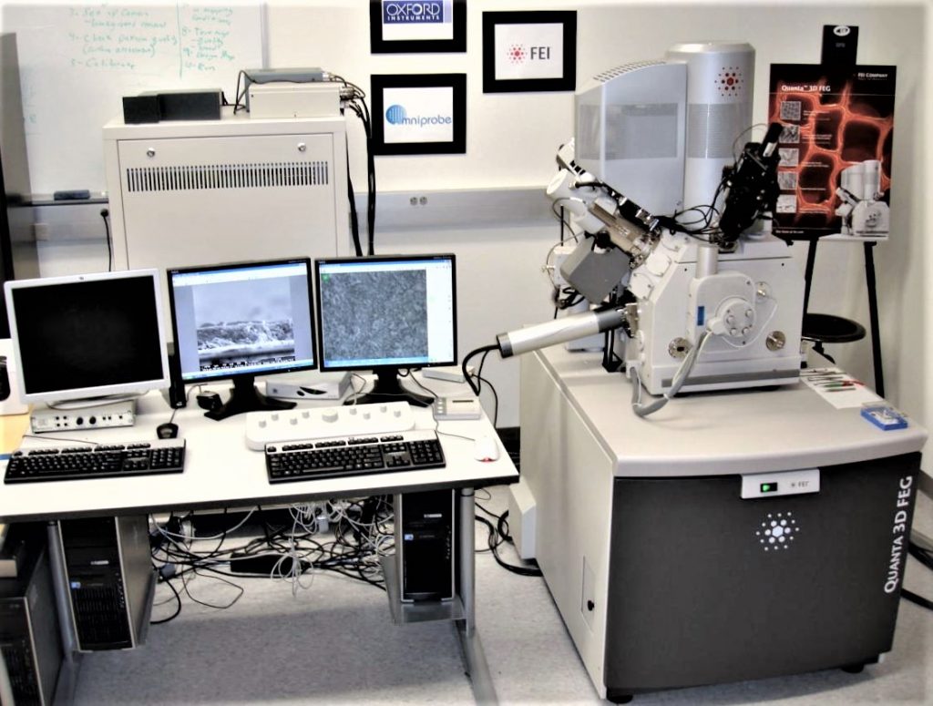
FEI Quanta 3D FEG Dual Beam (SEM/FIB)
| Location | 1302 Calit2 Building |
| Contact: | Dr. Ich Tran |
| Email: | ictran@uci.edu |
| EMERGENCY: | 9-1-1 |
| UCI Police: | (949) 824-5223 |
| UCI Medical Center: | (714) 456-6123 |
| Usage ($) | Training ($) | |
| UC Campuses |
451/302 | 40.00 |
| Other Academic |
58.51/392 | 52.00 |
| Industrial |
1351/902 | 120.00 |
NOTE: 1On-Peak rate. 2Off-Peak rate. Typical training time: 5 Hours. Training is billed per hour per person. Usage is billed per hour.
| Keycard Access: | Daytime or 24/7 |
| Instrument Access: | Daytime or 24/7 |
NOTE: Keycard access is required at all times to enter the TEM Labs. Users who have yet trained are not permitted to operate any lab instruments. Users who wish to bring guests are required to notify the Lab Manager in advance.
Description
The FEI Quanta 3D FEG is a state-of-the-art dual-beam (SEM/FIB) instrument. It is capable of high resolution surface imaging (1nm resolution at 30kV), fast composition analysis, crystal structure determination, orientation mapping, micromachining, Pt deposition, and TEM specimen preparation. It may be operated under three different vacuum modes: high vacuum, low vacuum and environmental (ESEM). Either dry inorganic samples or hydrated biological samples can be observed in this instrument.
Instrument Features
- Electron Source & Operating HT: Field emission gun 1kV~30kV
- Electron opticsHigh-resolution field emission – SEM column optimized for high-brightness/ high-current, 60 degree objective lens geometry with through-the-lens differential pumping and heated objective apertures
- Ion opticsHigh-current ion column with Ga liquid-metal ion source
Acceleration voltage: 2 – 30 kV
Probe current: 1 pA – 65 nA in 15 steps
15-position aperture strip
Magnification 40 x – 1280 kx in “quad” mode at 10 kV - Detectors and Attachments:
- Everhardt-Thornley SEDLow-vacuum SED (used in low vacuum)
Gaseous SED (GSED) (used in ESEM mode)
Solid-State BSED
Gaseous analytical BSED (GAD) (used for low-vacuum analytical applications)
EDS: Oxford silicon drift detector (50 mm2) and INCA software
HKL EBSD (Electron Backscatter Diffraction) systems - Additional capability:FP 2300/12 Peltier StageWhen cooled between 0 and 10 °C, specimens of very diverse nature can be imaged and analyzed at relative humidity conditions up to 100% (typical chamber pressures required are in the range 3-10 mbar). With the Peltier stage, humidity cycling experiments can be performed to characterize the sample’s morphology and phase distribution at various relative humidity conditions.In-situ freeze-drying can be performed when the temperature range of the Peltier stage is set below 0 °C with a minimum of –20 °C. The Peltier stage can also heat the sample up to ~60°C. The temperature and the ramp-up profile are directly controlled through the user interface of the microscope PC.
Popular Applications
- High-resolution SEM imaging with environmental control (HV, LV and ESEM)
- Specimen etching or deposition (FIB, GIS)
- Precise circuit modification/nanofabrication
- Micro/nano-scale patterning
- TEM sample preparation by combining FIB milling and Omniprobe lift-off process
- Elemental analysis and mapping (EDS)
- Crystallographic analysis and mapping (EBSD)
- Surface milling and automated milling scripts for micro-pillar patterns
- “Slice and View” SEM/FIB technique with video capability that allows for 3D reconstruction of a sample
Instrument Specifications
- Electron beam resolution:
- High-vacuum
1.2 nm at 30 kV (SE)
2.5 nm at 30 kV (BSE)*
2.9 nm at 1 kV (SE)
Low-vacuum
1.5 nm at 30 kV (SE)
2.5 nm at 30 kV (BSE)
2.9 nm at 3 kV (SE)Extended low-vacuum mode (ESEM)
1.5 nm at 30 kV (SE) - Focus Ion Beam resolution:7 nm at 30 kV at beam coincident point (5 nm achievable at optimal working distance)
| – | |
| — | – |
| — | – |
| — | – |
| — | – |
| — | – |
| — | – |
| — | – |
| — | – |
| — | – |
Useful Information
Instruction & Brochure
Application Notes
SOP & Safety Documents
Standard Operating Procedures